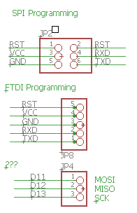
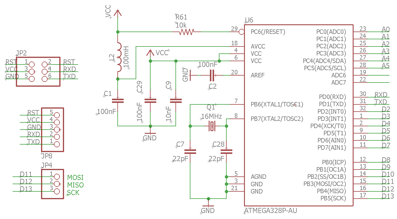
JP2 and JP8 are both serial pin headers suitable for programming -- they connect to the same pins of the chip: RXD, TXD and RST. This is programming via UART: A bootloader software (which has to be "pre-burnt" in the chip's flash memory) is the first thing that is run after a reset (RST) signal. It waits a little moment for data to arrive on RXD. If data arrives, the bootloader goes into programming mode: the data is written to flash memory, making it the firmware to be executed after the next RST. (If no data arrives: well, then the firmware that already is there is executed.)
Programming the chip via JP4 would use "hardware-supported" programming interface via SPI, recognizeable by the pins MISO, MOSI and SCK. That is the only way to get the first bootloader into the flash memory. It also provides you with a way to flash and re-flash a firmware without a pre-burnt bootloader (making the bootloader space available to your firmware). That method is described in the ATmega328P datasheet, chapter 27.8 and is the primary method employed by "ISP programmer boards". You could use those from the Arduino IDE using the menu option "Upload using programmer".
If this "barebone Arduino" circuit is meant to use an ATmega328P with the Arduino bootloader, however, I would assume that JP4 is meant to provide a pin header for some SPI sensor module (even though you could program and even un-brick the chip using this interface).
NB: "FTDI" is a red herring here. One of the most-used ISP programmer boards employs an chip made by FTDI, so you could call this method "programming via FTDI" ... but a specific USB-to-Serial cable using an chip made by FTDI and an 1x5 pin header is also called an "FTDI cable". (For a while, FTDI made the best USB-to-Serial chips. Clones just did not work that reliable. Today, CH340G and CP2104 are reliable enough for hobby projects, but somehow, "FTDI" stuck as a name.)


