I'm quite new to Arduino world and I'm trying to understand how shift registers work.
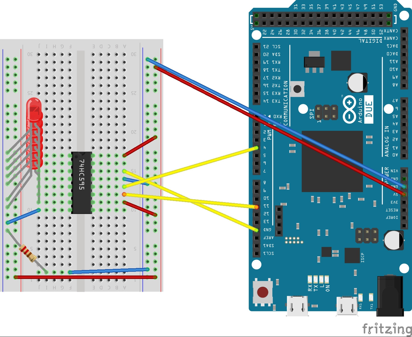
I built this construction :

In fact, it is an Arduino Duemilanove with AtMega on it, but afaik it doesn't matter.
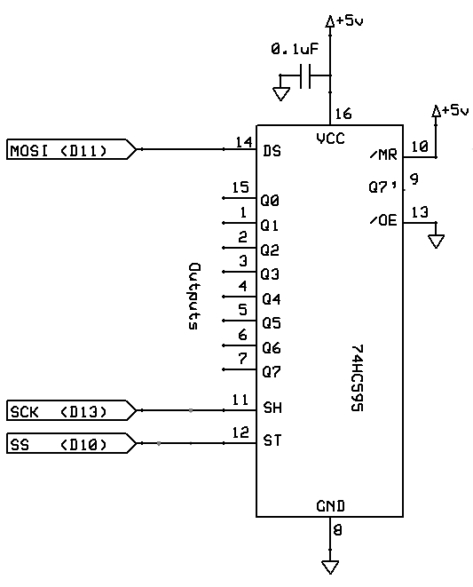
The tutorial I try to follow use SPI library so I try to do it too. I kind of understood that data input, latch and clock had to be pins 7, 4 and 11.
Basically, all I try to do is sending a byte to light the LEDs. As for me now, the sequence should light all LED, then no one, then one after another. I know there is one more input ont the right side of the SR but I didn't plan this model so I ran out of LEDs...
This is the code I use :
#include <SPI.h>
#include <StandardCplusplus.h>
#include <vector>
#include <iterator>
#include <size_type>

using namespace std;


//pin du shift register
#define DATA_PIN 13
#define LATCH_PIN 4
#define CLOCK_PIN 11
//à utiliser plus tard
#define INPUT_PIN 2


void setup() {
  pinMode(DATA_PIN, OUTPUT);
  pinMode(LATCH_PIN, OUTPUT);
  pinMode(CLOCK_PIN, OUTPUT);
  //pinMode(INPUT_PIN, INPUT);

  SPI.setBitOrder(MSBFIRST);
  SPI.setDataMode(SPI_MODE0);
  SPI.setClockDivider(SPI_CLOCK_DIV2);
  SPI.begin();

  //SPI.transfer(getBit(3));
  //digitalWrite(LATCH_PIN, HIGH);
  //digitalWrite(LATCH_PIN, LOW);

  Serial.begin(9600);
  Serial.println("start !");
}


void loop() {
  shift(B11111111);
  shift(B00000000);
  shift(B10000000);
  shift(B01000000);
  shift(B00100000);
  shift(B00010000);
  shift(B00001000);
  shift(B00000100);
  shift(B00000010);
  shift(B00000001);
}


void shift(int n){
  SPI.transfer(n);
  digitalWrite(LATCH_PIN, HIGH);
  digitalWrite(LATCH_PIN, LOW);
  Serial.print("shift : ");
  Serial.println(n);
  delay(1000);
}
When I upload this code, LEDs sequence has no sense, but serial output was totally OK.
What I see (without the output 0 of course) is : 1111111, 0111111, 1011111, 1110111, 1111101 and then 1111111 without further changes, whereas serial output is 255, 0, 128, 64, 32, 16, 8, 4, 2, 1, 255, 0, 128 and so on.
I assume I didn't understand something important, and it prevent me from finding answers in google.
Thanks for helping, it's really disturbing for me.
EDITS :
changed the title, it is a 74HC595.
Strangest behavior too (not gonna create another topic for that now), I dont have to connect both the gnd and VCC from my arduino for this to light LEDs. It changes a little the brighness of LEDs, but surprisingly VCC< GND< both
This is the tutorial I use to understand shift registers : https://youtu.be/6fVbJbNPrEU?t=195, and the one that uses SPI is nXl4fb_LbcI
I am now aware that I should get one resistor for each LED but I don't have that much resistors and as far as I can see this don't harm my LEDs nor underpower them.


#define DATA_PIN 13, #define LATCH_PIN 4statements. Maybe your other code compensates; but anyway fix it on your board and in your code and in your fritzing diagram then edit the question to match. I suggest you wire Ard pin 12 to '595 pin 12 and Ard pin 13 to '595 pin 13 to reduce cognitive dissonance. Also, wire pin 8 of the '595 directly to a ground bus, not to the LED bus that has a resistor between it and ground.I dont have to connect both the gnd and VCC from my arduino for this to light LEDs.- that is called "parasitic power" and it isn't good for the chip. Effectively the chip is being powered by the data inputs, which it is not designed to do.my LEDs don't die- not yet, no.