I am wary about providing a complete answer without knowing what is expected of YOU - is this like an assignment where you are being tested on understanding and what you have learned. The following will be useful to you. You need to give some more details if you want more assistance with these circuits.
Here is an existing stack exchange question. I see that I answered it in 2011 :-).
How does this power supply circuit work? (MCU + LM317)
The circuit and my previous answer should help greatly.
In your case you apply PWM using analog.Write to R1.
You MUST understand how the circuit works and not just apply it.
The original appears to be here with circuit description, with diagram here

On this page from EDN magazine is a similar circuit. The pot between pins 1 & 5 would not usually be used.

In another stack exchange question there is a very useful caution about the opamp's load limits in a similar circuit.
Problems controlling an LM317 with an op-amp - 2013
You can get many possible ideas here - search = lm317 voltage controlled power supply - this is an immensely powerful way of finding information - IF a picture is worth a thousand words then this is priceless. Note the terms used.
Bad designs:
There are some bad designs around which can look OK but behave badly.
Despite the detailed writeup,
This poor design uses "open loop control" and the output voltage varies with load and is only "sort of controlled".
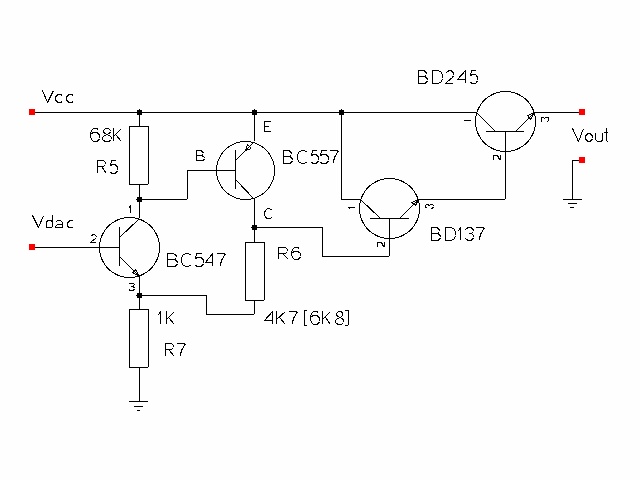
I was asked why I think this circuit is "open loop". I could not find a complete circuit diagram on the page but this diagram was shown of the output stage. If this is NOT the actual circuit used it would be "good" to have the complete circuit easily accessible.

IF this is the actual circuit used, then:
Call the transistors Q1 Q2 Q3 Q4 in left to right order.
Call intended output voltage = Vset = Vdac x (R6 + R7)/R7.
Vdac is applied to Q1 base and amplified by Q1 & Q2 to form the desired output voltage, appearing at Q2 collector. A lesser voltage appears as Vout due to the Vbe drop in Q3 & Q4. As load current increases Vout will "droop" thereby increasing the drive to Q4. This in turn increases the load on Q3 and Q3 emitter voltage will droop increasing Q3 drive. The actual Vbe voltages will depend on the beta (current gain) of Q3 and Q4, their temperatures (which depends on heat sinking, load and ambient temperatures) and manufacturing variation. At no or very low loads Vout will be about 1 Volt below Vset. At heavy loads Vbe_Q3 will be in the 0.6-0.8V range and Vbe_Q4 will be 0.8V+. So Vout will be around 1.5+ Volts below Vset and variable with (at least) the factors mentioned above.
This is still a usable design, but Vout could 'easily enough' be made far more stable with load by feedback from Vout to the Q1-Q2 amplifier - essentially forming a comparator that compares Vset and Vout.
Update:
This [reference provided by NilsB] MAY be the actual circuit diagram or close to it. It's an earlier 2005 design which presumably is much the same as the later version.

It appears not to be open loop in the broad sense. The Vout is still decoupled from Vset, with the software feedback allowing him to adjust the Vset to make Vout what he wants on a "nudge it and see" basis. ie Vset is not a fixed ratio wrt Vout so he can never set it and have it "just track". So it does not automatically stabilise for load or temperature changes and there is a variable drp between k x Vset and Vout.
Software is fastish but not as fast as a closed loop in hardware which allows Vout to track Vset within mV in a time delay as short as you provide an error amp loop for.
That's a 2005 circuit diagram so an earlier version than the originally cited V3 - one assumes he has not 'gone backwards' in design concept. It's strange that he does not include the whole circuit diagram or a good discussion of the provided current and voltage feedback. He may have wanted to sell kitsets rather than give away his final design. The link to the kitset sales is now broken so he now manages neither.
I'd consider it preferable to add a simple hardware error amplifier so Vout = k x Vset and THEN measure Vout and Iout with ADCs (as he does). Vout is then essentially "set and forget" with the added ability to check that Vout is what it should be (which allows eg heavy overload to be detected.
Constant current mode operation is still "nudge and see" but 'not too bad'.
Also, Vout includes the Vdrop across the current sense resistors - about 0.5V/A. Measuring with 2 x AD C channels as he does allows this to be compensated for. If the Isense resistors were in the "high side" feed before the regulator this would remove this variation but make current sensing somewhat harder.


